So my fun task for this time is to find out how to program TI TrxEB LCD. So I started by understanding the wiring on the board and finding out which msp430 ports I need. Below is the result depicted:
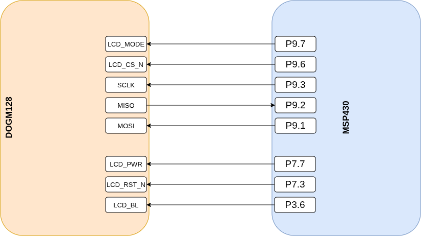
Simplified wiring diagram.
Knowing that so mainly we need to do these steps:
- Find the SPI settings expected by the LCD
- Find the configuration register values of the LCD
- Setup SPI accordingly on the MSP430
- Write the LCD configuration registers over spi
- Write any test string
So i have done all that and here my code. So first of all we need to configure the clock for spi. 4 MHz or 8 MHz should be fine. Here how to get it:
  PMMCTL0_H = PMMPW_H;              // Unlock PMM registers
  PMMCTL0_L |= PMMCOREV_1;          // Set VCore to 1.6V (Supports up to 12MHz)
  PMMCTL0_H = 0x00;                 // Lock PMM registers
  UCSCTL3 |=SELREF_2;               //fll ref = REF0 (32.768 K)
  UCSCTL4 |= SELA_2;                // ACLK = REFO
  UCSCTL4 &= ~(SELS_7 | SELM_7);    // Clear select bits
  UCSCTL4 |= SELS_3 | SELM_3;       // SMCLK = DCOCLKDIV, MCLK = DCOCLKDIV
  __bis_SR_register(SCG0);          // Disable FLL control loop
  UCSCTL0 = 0x0000;                 // Reset DCO/MOD
  UCSCTL1 = DCORSEL_4;              // Range 4 (up to 16MHz)
  // N = 121 -> ~4 MHz
  UCSCTL2 = FLLD_0 + 121;
  __bic_SR_register(SCG0);          // Re-enable FLL
  __delay_cycles(256000);
  // 4. Clear Fault Flags
  do {
      UCSCTL7 &= ~(XT2OFFG | XT1LFOFFG | XT1HFOFFG | DCOFFG);
      SFRIFG1 &= ~OFIFG;
  } while (SFRIFG1 & OFIFG);
  // 5. Select DCO for SMCLK and MCLK
  UCSCTL4 = (UCSCTL4 & ~SELS_7) | SELS__DCOCLK;
  UCSCTL4 = (UCSCTL4 & ~SELM_7) | SELM__DCOCLK;
So now we configure SPI bus and use the 4 MHz for it:
 P9SEL    |= BIT1 | BIT2 | BIT3;
 UCB2CTL1  = UCSWRST;
 UCB2CTL0  = UCCKPH | UCMSB  | UCMST | UCSYNC;
 UCB2CTL1 |= UCSSEL__SMCLK;
 UCB2BR0 = 1; //clk divider so 4 MHz/1
 UCB2BR1 = 0;
 UCB2CTL1 &= ~UCSWRST;
 P9DIR |= BIT6 ; //LCD_CS_N active low
Power up the LCD an reset it:
//Power
P7SEL &= ~BIT7;
P7DIR |= BIT7;
P7OUT |= BIT7;
//Reset
P7DIR |= BIT3;
P7OUT &= ~BIT3;
__delay_cycles(600000);
P7OUT |= BIT3;
Now we start writing to LCD registers, first we configure it:
  P9OUT &= ~BIT6;      //CS low start transmission
  // Configure P9.7 to control lcd mode (cmd or data)
  P9SEL &= ~BIT7;
  P9DIR |= BIT7;       // Output
  P9OUT &= ~BIT7;      // low = cmd
  __delay_cycles(50000);
  SpiWrite( 0x40); /*Display start line 0                    */
  SpiWrite( 0xA1); /*ADC reverse, 6 oclock viewing direction */
  SpiWrite( 0xC0); /*Normal COM0...COM63                     */
  SpiWrite( 0xA6); /*Display normal, not mirrored            */
  SpiWrite( 0xA2); /*Set Bias 1/9 (Duty 1/65)                */
  SpiWrite( 0x2F); /*Booster, Regulator and Follower On      */
  SpiWrite( 0xF8); /*Set internal Booster to 4x              */
  SpiWrite( 0x00); /*                                        */
  SpiWrite( 0x27); /*Contrast set                            */
  SpiWrite( 0x81); /*                                        */
  SpiWrite( 0x16); /* <- use value from LCD-MODULE .doc guide*/
                      /*    for better contrast (not 0x10)      */
  SpiWrite( 0xAC); /*No indicator                            */
  SpiWrite( 0x00); /*                                        */
  SpiWrite( 0xAF); /*Display on                              */
  SpiWrite( 0xB0); /*Set Page 0                              */
  SpiWrite( 0x10); /*High-Nibble of column address           */
  SpiWrite( 0x00);  /*Low-Nibble of column address            */
  __delay_cycles(100000);
  SpiWrite( 0xA5);
  __delay_cycles(100000);
  SpiWrite( 0xA4);
  spi_uscib2_cs_high();
  __delay_cycles(10000);
  P9OUT |= BIT6; CS high stop transmission
The LCD is now configured and ready to be printed:
// helper function to navigate the screen,
void gotoXY(unsigned char x, unsigned char y)
{
    unsigned char cmd[] = {0xB0, 0x10, 0x00};
    cmd[0] = cmd[0] + y;
    cmd[2] = cmd[2] + (x & 0x0F);
    cmd[1] = cmd[1] + (x >> 4);
    SpiWrite(cmd[0]);
    SpiWrite(cmd[1]);
    SpiWrite(cmd[2]);
}
//Print some lines on the screen
 uint8_t lineFill = 0x00;
// the lcd has 8 lines in each 128 clmns
 for (int yIdx =0;yIdx<8;++yIdx)
 {
   LCD_gotoXY(0, yIdx);
   P9OUT &= ~BIT6;
   P9OUT |= BIT7;      // data mode
   for (int i = 0; i < 128; i++)
   {
      while (!(UCB2IFG & UCTXIFG));
      UCB2TXBUF = lineFill;
      while (UCB2STAT & UCBUSY);
   }
   if (yIdx%2 !=0)
     lineFill = 0x00;
   else
     lineFill = 0xFF;
 }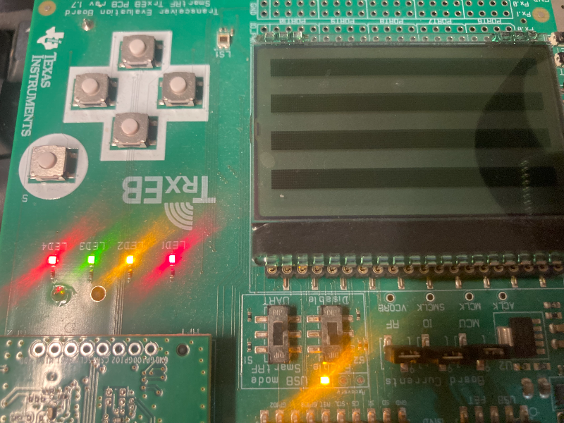
So finally you should see something like this. During configuring the LCD i saw a noise pattern on it for a short time. May be you know why? 🤔
Subscribe to get last updates.
